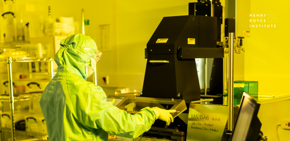
This recently upgraded UV Mask Aligner Lithography Tool is a Suss MA/BA6 used in the process of transferring a design such as a CAD or GWL file, or a ready to use mask, onto a substrate coated in photoresist; a material essential for the lithography process.
After chemical development, subsequent steps allow for the deposition, or removal via etching, of materials within that pattern. This process is repeated to allow for the creation of a device layer by layer.
This allows for the fabrication of devices such as;
- Bioelectronic devices
- MEMS energy harvesters
- microelectronic devices
- patterned electrodes for batteries or solar cells.
The benefit of a UV lithography tool over a laser writer or electron beam lithography system is the speed of the process. Once aligned the system is capable of exposing a 6 inch wafer in less than 30 seconds. Recently upgraded the system uses an LED light for increased stability of the light source which boosts reproducibility. This reduces the use of Nitrogen to cool the system enabling a more sustainable approach.
This UV Lithography Tool can manufacture devices with a minimum feature size over 700 nm. It can process substrates ranging from millimetre-sized samples up to a maximum substrate size of 6 inches in diameter.
For devices that require multiple layers; the system is capable of an alignment accuracy of 250 nm.
All operations are fully automatic, with software-controlled optics and wafer chuck. This allows for the automation of wafer edge compensation when loading a substrate. This system features a video-assisted self-alignment function for pattern recognition of alignment marks.
The tool allows exposure in several contact modes: proximity, soft, hard, and vacuum. The long-focal optics are suitable for processing either thin (high-res) or thick (e.g. SU8) photoresists.
If your research interests require you to pattern wafers, please contact Facility Manager Sue Murkett (sm330@cam.ac.uk) at the Nanoscience Centre cleanroom.
