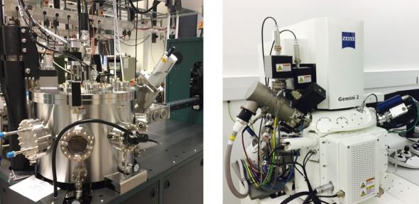
The Royce Physical Vapour Deposition and Materials Characterisation Facility includes eight UHV sputter deposition systems, two pulsed laser deposition chambers and a UHV electron beam evaporator for the automated growth of metallic and oxide heterostructures for devices. It also has a Zeiss Cross-beam 540 focused ion beam/electron beam system (FIB-SEM) for in-situ patterning and device fabrication. It can operate with the sputtering MBE capability of the Royce PVD suite.
Some sputtering chambers include load-lock entry for rapid materials growth and the AJA system is configured with 11 targets, internal calibration and automated processes for the growth of complex metallic or insulating heterostructures for devices. This facility provides a unique capability for 3D heterostructure fabrication which can generate novel magnetic and optical materials systems.
The dual beam FIB-SEM system uses a range of ion sources. This includes a Ga ion beam to enable direct patterning of micro-pillar and nano-pillar devices. It also offers an alternative to the standard subtractive etch process used in optical lithography. This system can produce devices on a smaller scale without breaking vacuum, and without forming ex-situ interfaces.
As a combined suite, the sputtering and FIB systems offer the capability for 3D heterostructure device fabrication for magnetic and optical materials systems.
For more information about characterisation of your materials and devices, or using Physical Vapour Deposition (PVD), patterning and growth of metallic structures for devices, contact Professor Jason Robinson (jjr33@cam.ac.uk) or Dr Nadia Stelmashenko (nas19@cam.ac.uk) in the Department of Materials Science and Metallurgy.
