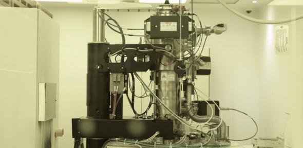
Our Electron-Beam Lithography System is a Raith EBPG 5200 capable of device fabrication at the nanometre scale. This state-of-the-art system combines best-in-class lithography performance with high-throughput and full automatisation.
The equipment’s electron-optics performance allows fabrication of features as small as 5nm. It’s equipped with a thermal field emission gun operating at 100 kV, reducing proximity-effect related difficulties and enabling high aspect-ratio patterning.
The system has a fast arbitrary-shape pattern generator with a maximum clock rate of 125MHz. This enables a high throughput especially for novel metamaterial devices, making the EBPG the fastest tool for high-density patterning.
This lithography tool handles industry standard semi-conductor wafers up to 200 mm (8 inch) and 7 inch photomask blanks. The system is compatible with a broad range of semi-conductor and dielectric substrates:
- Silicon
- III-V Semi-conductors
- Glass, quartz and dielectrics
Accurate feature sizing and placement is derived from the tool’s precision interferometer stage. The overlay of subsequent pattern layers can be better than 10nm.
The system contributes to the development of:
- novel nano-electronic devices
- on-chip integrated optoelectronic circuits
- quantum devices
- layered material related devices
- photonic and plasmonic systems
The system initially enables the fabrication of research scale prototype devices. Once completed, processes can be scaled up towards larger-scale production. This forms the bridge between university research and wafer-scale manufacturing.
The Electron-Beam Lithography Facility is fully staffed with experienced nanofabrication scientists who can lead the design process for your devices and advise on best manufacturing practices. The system is readily available and can work to your required timescales.
If your research interests or manufacturing needs require use of an Electron-beam Lithography tool please contact the Collaborative R&D Environment (CORDE) at the Department of Physics or contact Facility Manager Jon Griffiths (jpg35@cam.ac.uk).
