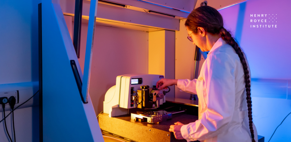
The Bruker Dimension Icon Pro is a scanning probe microscopy system with a stage which holds samples up to a 200 mm (8-inch) wafer, with all points on the stage accessible without wafer rotation. Semi-automated mapping is available. For atomic force microscopy (AFM) topographic measurements, the noise floor is 0.3 Angstrom.
Typical uses of the system include topographic measurements of semiconductor materials, particularly GaN, with imaging of monolayer steps and quantification of extended defect densities being routine. Electrical modules are used to identify unintentionally doped regions and the impact of detects on local electrical properties. TUNA and KPFM are used, comparing data with and without illumination, to reveal inhomogeneities in perovskite solar cells. Multiple projects address 2D materials, including their impact on composite structures, with TUNA and FFM being used to address electrical and mechanical properties respectively in this context.
Topographic measurements may be performed in contact mode, tapping mode or PeakForce tapping mode, and in-built materials property measurement modes include Kelvin probe force microscopy (KPFM), magnetic force microscopy (MFM), piezo-response force microscopy (PFM), friction force microscopy (FFM), phase imaging and quantitative nanomechanical mapping (QNM).
The system is also equipped with modules for scanning capacitance microscopy (SCM), scanning spreading resistance microscopy (SSRM), and extended tunneling AFM (TUNA) which accesses the current ranges for both standard TUNA and conductive AFM (CAFM). It is equipped with a 1 sun light source which allows illumination of transparent samples from the back side during measurement, for photo-conductive AFM and measurements on light-sensitive samples.
If your research interests require characterisation of your materials or devices using wafer scale AFM, or you would like to discuss opportunities for such characterisation using the AFM Scanning Probe Microscopy Suite please contact Facility Manager Prof Rachel Oliver (rao28@cam.ac.uk) in the Department of Materials Science and Metallurgy.
