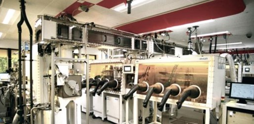
The ambient processing cluster tool is a custom-built glovebox cluster tool that integrates different vacuum as well as liquid-based deposition technologies for a wide range of functional materials into a common inert glove box atmosphere. It comprises ten glove box modules that are interconnected by a semi-automated inert atmosphere transfer system and includes tools such as thermal evaporation, sputtering, pulsed laser deposition (PLD) and atomic layer deposition (ALD) as well as aerosol printing, screen printing and slot-die coating. The tool also includes modules for metrology, thin film encapsulation and packaging. The tool gives access to a wide range of functional materials, including transition metal oxides for battery and other applications, organic and hybrid organic-inorganic semiconductors, two-dimensional materials, polymer composites etc.
Its unique configuration allows integration of these different classes of materials into novel hetero-architectures and but also fabrication of a wide range of devices including solar cells, batteries, mechanical or thermoelectric energy harvesters as well as integrated energy systems for energy–efficient ICT applications. The Cluster Tool has been designed with all the features that enable clean sample fabrication.
If your research interests require controlled deposition of any of the above materials or you would like to combine functional materials in novel ways and have any questions on the tool’s capabilities please contact the academic lead Professor Henning Sirringhaus (hs220@cam.ac.uk) or the technical lead Steve Haws (sah219@cam.ac.uk) in the Department of Physics.
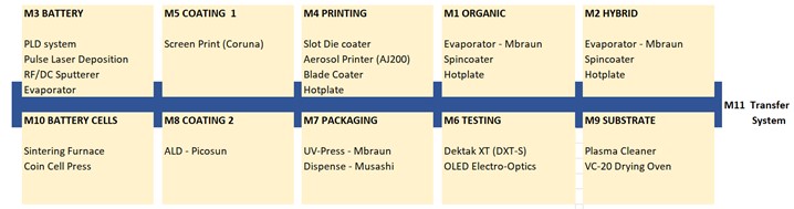
There are ten glovebox modules that comprise of (click to view):
Electrochemical and Energy Storage Test Equipment
The electrochemical quartz microbalance with Low Current Potentiostat tool comprises a Q-sense Explorer system with QE 401 electronics unit, a Q-sense chamber platform a Q-sense flow module and a Q-sense electrochemistry module (http://www.biolinscientific.com/product/q-sense-explorer/). This is combined with a Bio-Logic SP-200 potentiostat/galvanostat with Electrochemical Impedance Spectroscopy and Ultra Low Current (http://www.ec-lab.co.uk/sp-200-sp-240-new-research-grade-potentiostat.html).
This system provides the capability to characterise the changes in mechanical properties and mass of thin film materials during electrochemical cycling, chemical reactions or phase changes. Film thicknesses can be from <1nm to several microns depending on material. The EIS capability provides characterisation of diffusion processes within electrode materials or other electrochemical systems. Overall, it provides capability for mechanical characterisation of a wide range of material systems including battery materials, supercapacitor materials, thermoelectric materials and thin film materials for ICT applications.
If your research interests require measurement of the mechanical changes of thin film materials during electrochemical cycling, reactions, phase changes or to discuss your experimental needs, contact academic lead Professor Clare Gray ( cpg27@cam.ac.uk ) in the Department of Chemistry.
This module is designed to produce organic semiconducting devices such as organic LEDs, organic solar cells, OFETs and thermoelectrics. New device structures often require the combination of different preparation methods. The deposition of the required thin film can be realised by solution-based processes, or via physical vapour deposition under vacuum conditions.
The system is split into two sections, one section is dedicated to solution processing, the second is for vacuum deposition of organic and metal layers. The evaporator allows (co-)evaporation of organic molecular compounds, inorganic compounds (e.g. MoOx, LiF) and/or metals (e.g. Au, Al, Ag). While metals and inorganic compounds can be simply evaporated using thermal sources (boat-type or effusion cells) under high vacuum conditions, organic compounds must be evaporated with special care. Precise temperature control over a wide temperature range is combined with a special source design to allow deposition of organics.
The spin-coater may be programmed to modify recipes of multiple steps, and may operate over a wide parameter range (speed, acceleration, deceleration etc. may be carefully controlled). Complex devices where various solvents were used in deposition will benefit from a regenerable solvent vapour removal system integrated in the glove box purification system, to ensure a contamination-free environment.
Organic Vacuum Thermal Evaporator Specifications:
| Two High Temperature Metal Sources: | up to 1800°C |
| Four Lower Temperature (ceramic pot) Sources: | up to 800°C |
| Substrate size: | up to 99mm x 99mm |
| Custom Inlays: | allow for matrix of smaller sizes within maxium |
| In-situ mask changing: | to enable layered structures with shadow masking under vacuum |
| High Vacuum Side Pressure: | ultimately down to 1E-8 mbar |
| Rate Sensor Heads (QCM): | 4 independant |
| Substrate Temperature: | up to 300degC |
| Temperature Control of the Crucible: | precision of < ±0.1 K |
| Co-Depositions: | up to 4 for complex stochiometrics |
| Substrate Rotation: | 0 to 30 rpm |
Spin Coater Specifications:
| Max Spin Speed: | 10,000 rpm |
| Substrate Size: | up to 100 x 100mm |
Designed to handle and deposit potentially hazardous materials like (e. g. Methylammonium halides, Lead Iodine, Lead Bromine, Caesium Iodine, etc.)
The hybrid module is designed to produce combinations of organic semiconductors, polymer nanocomposites and hybrid organicinorganic semiconductors, such as metal halide perovskites. And can handle precursors such as MAI (Methylammonium iodide), PbCl2 and PbI2 for perovskite solar cells. The system is split into two sections. One section is dedicated to solution processing, the second is for vacuum deposition of layers in a special PVD system. The evaporator enables deposition of perovskite solar cells and organic/inorganic FETs. The spin-coater may produce films from a solvent based source, and the hotplate is used to drive off the solvent fraction from a coated film.
Hybrid Evaporator Specifications:
| (1 off) ULTE: | Ultra Low Temperature sources: -10 to 250degC +/- 0.1K |
| (3 off) LT: | Low Temperature ceramic sources: 50degC to 800degC +/- 0.1K |
| Typical deposition rates: | up to 5 Å/sec at throw distance 150 mm |
| (2 off) Metal boat sources: | up to 1800degC |
| Al Evaporation: | Custom ceramic pot configuration for Al evaporation |
| Typical deposition rates for Aluminium: | Up to 20 Å/sec at throw distance 250 mm |
| Substrate size: | up to 100x100mm with frames allowing for partitioning, eg into 3x3x matrix of 1x1inch |
| Substrate temperature: | Heating / cooling from room temperature to 300°C |
| High vacuum side pressure: | ultimately down to 1E-8 mbar |
| Control: | Sophisticated computer process control. Remote operation via Teamviewer |
Hybrid Spincoater and Hotplate Specifications:
| Substrate size: | up to 100 x 100mm |
| Spin speed: | up to 10,000 rpm |
| Hotplate temperature: | controllable up to 200°C |
This module supports deposition of sputtering of battery electrodes and solid electrolytes. With multi-source target arrays, metals and metal oxides can be deposited to form, for example, lithium ion batteries and supercapacitors. It can quickly achieve base pressure of 5 x 10⁻⁷ mbar and enables deposition of relatively thick films of transition metal oxides for cathodes and solid-state electrolytes. The module is run under an argon atmosphere.
The module consists of: the Pulsed Laser Deposition system (PLD) that has a single and twin beam configuration to allow co-deposition and stoichiometric tuning; and the DC/RF sputterer that can be run in a variety of gas ambients to influence stoichiometry of the deposited material. Typical material depositions include metals and transition metal oxides
The systmes can produce a thermal ramp of substrates up to 20 °C/min to 500 °C and 10 °C/min from 500 to 1000 °C, and has six locations for 1 inch diameter, 6mm-thick targets. The system can achieve up to 4 J/cm2 laser fluence with 20 nm pulses, 28 MW power per pulse, maximum power of 700 mJ, and pulse repetition rates of up to 10 Hz. Process recipes can be programmed to allow automated running of processes. The evaporator can accommodate a wide range of materials due to a PID-controlled source temperature up to 1200 °C, and has an integral link to the sputterer to enable sequential operations without breaking vacuum. The sputterer is for deposition of metals and transition metal oxides for battery construction, with two DC and RF sputter target positions.
Pulsed Laser Deposition Specifications:
| Configuration: | Single and Twin Beam |
| Fluence: | Up to 4J/cm2 |
| Pulse Time: | 20ns |
| Pulse Power: | up to 28 MW |
| Maximum Energy: | 700mJ |
| Pulse repetition: | up to 10 Hz |
| Substrate Size: | Maximum 10 x 10mm |
| Substrate Temperature: | Up to 1,000 oC |
| Temperature Ramp Rate: | up to 20 oC/min to 500 oC, then 10 oC/min to 1,000 oC |
| No. of Target Locations: | 6 |
| Target thickness: | 6mm |
| Automation: | Programmable for automated running |
| Availible Gases: | Ar and O2 |
Sputterer Specifications:
| Substrate size: | Single substrate @ maximum 10 x10 mm |
| Power: | Up to 30W |
| Targets: | 2 DC and 2 RF, 1.3 inch diameter |
| Available Gases: | O2, N2 and Ar |
Sputterer Specifications:
| Substrate size: | Single @ maximum 10 x10 mm |
| Temperature: | up to 1,000 oC |
| Source: | single source, graphite pot |
Aerosol printing allows a wide range of materials, including silver, to be deposited in fine and complex patterns down to 11 μm resolution using a suitable ink precursor. Device structures including small contact pads can be created and aligned to previous layers.
The slot-die coater allows pin-hole free films to be deposited, for example the deposition of encapsulating materials to seal solar cell devices from moisture and air and also thin polymer dielectrics. Compatible materials include a wide variety of inks, pastes, or metals, conductors, insulators, ferrites, and polymers.
The blade coater is a small unit for the formation, by coating, of test structures and devices.
Aerosol Printer Printer Specifications:
| Resolution: | down to 11µm |
| Motorised (X/Y) Platten size: | 6x6 inch |
| Ultrasonic for: | 1 to 10 cP |
| Pneumatic for: | 1 to 1000 cP |
| Work to date includes: | silver ink, transition metal oxides and nanoscale ITO |
| Droplets size: | Rranging from 1 to 5 µm in diameter |
Slot-Die Coater Specifications:
| Deposited Thickness: | Thin 100nm eg dielectric layers up to thick, – 10 microns for eg encapsulation with polyimide |
| Vacuum Platen Size: | Supports device substrates of up to 8x12 inch (with smallest 200mm x 3mm prime plate) |
| Platen Heating: | to 80 °C |
| Nozzle (die lips): | height adjustable to resolution of 1um |
Blade Coater Specifications:
| Maximum trace width: | 3cm |
| Maximum trace length: | 5cm |
This affords high resolution and high precision patterning of pin-hole free patterns to support the definition of device structures on a range of substrates, including glass and plastic film. This includes multiple-print processes, stacking, wet-dry, dry-wet and limited micro gap printing. Many different base substrates can be printed on, including ceramics, silicon wafers, foils and paper.
High Resolution Screen Printer Specifications:
| Max. Substrate Size W(X) x L(Y) x H(Z): | 200x200x12mm Max. |
| Print Size (Image size): | 180x180mm Max. |
| Table Movement (X/Y): | 100mm |
| Table Sensitivity (X/Y): | 1µm |
| Table Repeatability: | +/-2µm |
| Layer to Layer Alignment: | < +/- 10µm |
| Max. Table Rotation: | (A) +/- 5° (Fine) / 360° (Rough), Sensitivity (A) 20 arcsec |
| Max. Print Length (Left/Right): | 305mm |
| Max. Print Width: | 180mm |
| Squeegee variations: | Squeegee/Sqeegee, Sqeegee/Flood Squeegee |
| Sqeegee Movement: | Manually |
| Sqeegee Guiding: | Twin Guiding, Level adjustable |
| Squeegee Down/Up: | Manually by handle |
| Camera System MicroscopW: | Camera 50-500x (2000x Digital) |
| Camera Resolution: | 5MP |
| Monitor LCD: | , 2 Pieces 3.5“ (89mm) |
| Ilumination: | Incident LED Light |
The profilometer can measure the height of features from around 50 nm to 150 μm. Surface roughness can be measured to sub-nm levels, supporting the characterisation of film morphologies. Whether measuring thicknesses to obtain critical values for device simulation or for process control, such measurements are vital for the range of deposition techniques used in battery, solar cell, TFT and OLED architectures.
Dektak Specifications:
| Height resolution: | Less than 10nm |
| Repeatability: | down to 4A |
| Substrates size: | up to around 6 inch wafer size |
| Operating Modes: | Low force for sensitive materials |
This allows a range of UV-curable types of sealant beading to be precision-deposited for subsequent UV curing in the press. This module supports effective encapsulation, vital for many solar cell architectures.
Encapsulation Specifications:
| Substrate Size: | 1 x1 inch |
| Coverslip Size: | Custom |
| Sealing: | Perimeter or flood sealing via combined pressure & UV exposure |
| Capacity: | 9 devices at a time |
| Ca Test: | 5 days with perimeter seal |
ALD affords exceptional conformal deposition of oxides in monolayer-by-monolayer precision. This allows very effective encapsulation of a device structure, and also allows fabrication of the highest quality dielectrics for capacitor and TFT structures.
ALD Specifications:
| Precursors: Currently for: | TiO2, Al2O3, HfO, SnO2 (option to switch in others) |
| Uniformity: | 0.6% single sigma across 8 inch wafer with Al2O3 |
| Substrate size: | 8 inch platen for any sizes that will fit in this area |
| Temperature: | substrate temperaures up to ~ 400°C |
| Temperature Sensitive Substrates: | For temperature sensitive substrates Al2O3 process proven down to 75°C and SnO2 down to 100°C |
Plasma ashing of surfaces is an established technique for promoting adhesion of a subsequent coating, through enhancement of surface wetting characteristics by the removal of organic surface contaminants. The vacuum oven can be used with low heat to evaporate off the solvent component of a deposited layer, and may be operated without heat for temperature-sensitive systems. Such treatment can be important in the preparation of a surface for subsequent material depositions.
O2 Plasma Asher Specifications:
| Power: | Maximum 300 W |
| Configuration: | Roughly 2 x 4 inch diameter (or smaller) substrates can be accommodated |
| Gases: | O2 as standard with optional use of Ar |
Vacuum Oven Specifications:
| Capcaity: | Approx. 8 x 8inch with two trays |
| Temperature: | 200°C |
| Gases: | Bleed valve allows partial pressure under dry N2 flow |
This glovebox module comprises a high temperature furnace for sintering of materials and a crimping press for the sealing and unsealing coin cell batteries.
Furnace Specifications:
| Internal Chamber Size: | 120 x 120 x 120 mm |
| Maxiumum Temperature: | 1,400°C |
| Operation: | For non-evaporating materials only |
Coin Cell Crimper Specifications:
| Mode: | Manual Operation |
| Cell Size: | Compatible with CR20XX coin cells |
| Operation: | Exchangeable mould for crimping as well as de-crimping of coin cells |